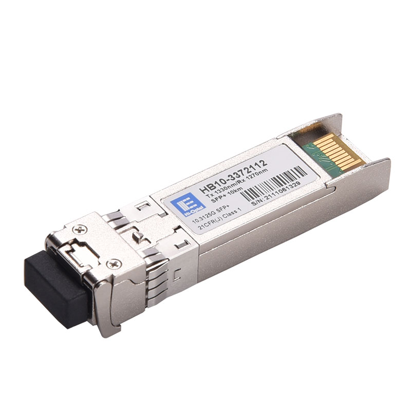
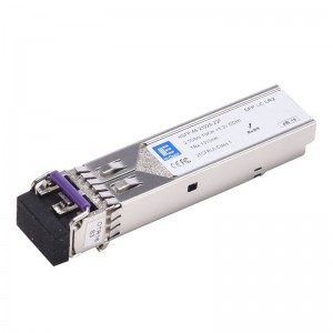
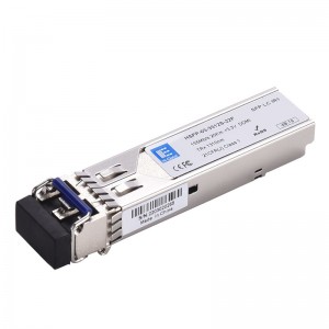
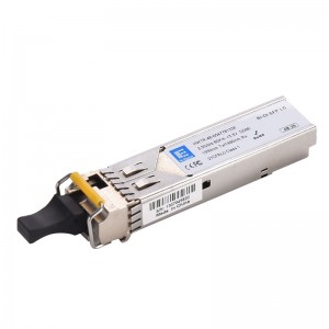
10GBASE-BX SFP+ 1330nm-TX 1270nm-RX 10km Hi-Optel HB10-3372112 module
Description
The transceiver consists of two sections: The high performance a 1330nm DFB Laser, Transmitter and high sensitivity PIN integrated with a TIA. Receiver.

The module is hot pluggable into the 20-pin connector. The high-speed electrical interface is based on low voltage logic, with nominal 100 Ohms differential impedance and AC coupled in the module. The optical output can be disabled by LVTTL logic high-level input of TX_Disable. Loss of signal (RX_LOS) output is provided to indicate the loss of an input optical signal of receiver. The receiver RATE_SELECT pin is not used by the transceiver.
A 2-wire interface (SCL, SDA) is used for serial ID, digital diagnostics and other control /monitor functions.
Applications
● LTE optical repeater application,other optical links
● 10G Base- LR/LW
● Other optical links
Standard
● Compliant with SFF-8431 and SFF-8432
● Compliant with SFF-8472 Rev 10.2
● Compliant with IEEE 802.3ae 10GBASE-LR and 10GBASE-LW
● RoHS Compliant
Absolute Maximum Ratings
|
Parameter |
Symbol |
Min |
Max |
Unit |
| Storage Temperature |
TST |
-40 |
+85 |
℃ |
| Supply Voltage |
VCC3 |
0.0 |
+3.6 |
V |
| Relative Humidity |
RH |
5 |
95 |
% |
Recommend Operation Environment
|
Parameter |
Symbol |
Min |
Typ |
Max |
Unit |
|
Date Rate |
10.3125 |
Gb/s |
|||
|
Supply Voltage |
VCC |
+3.14 |
3.3 |
+3.47 |
V |
| Supply Current |
ICC |
300 |
mA |
||
| Power Dissipation |
PD |
800 |
1000 |
mW |
|
| Operating Temperature |
TOP |
0 |
25 |
+70 |
℃ |
Electrical Characteristics (Condition: Ta=TOP)
|
Parameter |
Symbol |
Min |
Typ |
Max |
Unit |
Note |
||
| Transmitter | ||||||||
| Differential input voltage swing |
VI |
150 |
1600 |
mVpp |
1 |
|||
| C common mode voltage tolerance |
15 |
- |
- |
mV |
||||
| Transmit Disable Input |
H |
VIH |
2.0 |
Vcc+0.3 |
V |
|||
|
L |
VIL |
0 |
0.8 |
V |
||||
| Transmit Enable Output |
H |
VOH |
2.4 |
Vcc+0.3 |
V |
|||
|
L |
VOL |
0 |
0.4 |
V |
2 |
|||
| Data Dependent Input Jitter |
DDJ |
0.1 |
UI |
|||||
| Data Input Total Jitter |
TJ |
0.28 |
UI |
|||||
| Input Differential Impedance |
Zin |
80 |
100 |
120 |
Ω |
|||
| Receiver | ||||||||
| Differential output voltage swing |
500 |
700 |
mVpp |
3 |
||||
| LOS Output |
H |
VOH |
2.4 |
Vcc+0.3 |
V |
2 |
||
|
L |
VOL |
0 |
0.4 |
V |
||||
| Rx Output Rise and Fall Time |
Tr/Tf |
30 |
ps |
20% to 80% |
||||
| Total Jitter |
TJ |
0.7 |
UI |
|||||
| Deterministic Jitter |
DJ |
0.42 |
UI |
|||||
| Output Differential Impedance |
Zon |
80 |
100 |
120 |
Ω |
|||
Note 1) TD+/- are internally AC coupled with 100Ω differential termination inside the module.
Note 2) Tx Fault and Rx LOS are open collector outputs, which should be pulled up with 4.7k to 10kΩ resistors on the host board. Pull up voltage between 2.0V and Vcc+0.3V.
Note 3) RD+/- outputs are internally AC coupled, and should be terminated with 100Ω (differential) at the user SERDES.

