400G QSFP-DD DR4 Optical Transceiver HQSFPDD-1L2 1310nm EML,PIN, 0~70℃
Features
● QSFP-DD MSA rev 5.1 compliant l
● 802.3bs compliant
● QSFP-DD-CMIS-rev4p0
● 400GE DR4 Specification compliant
● 8 x 53.125 Gbit/s PAM4 electrical interface (400GAUI-8)
● Non-hermetic package design
● Maximum power consumption 12 W
● MPO connector
● 425 Gbit/s aggregate bit rate
● Up to 500 m transmission on single mode fiber with FEC
● Operating case temperature: 0℃~70℃l
● Single 3.3 V power supply
● RoHS-2 compliant
Applications
● Data center network
General Description
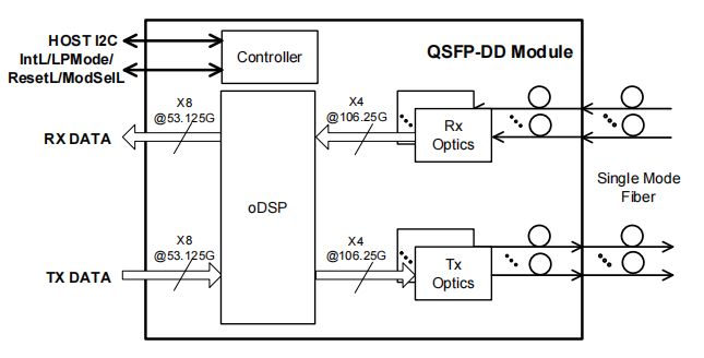
HQSFPDD-1L2 is a transceiver module designed for 500 m optical communication applications, and it is compliant with QSFP-DD MSA, IEEE 802.3bs protocol and 400GAUI-8 standards. The 425 Gigabit signal is carried over four parallel lanes by one wavelength per lane. This module can convert 8-channel 53.125 Gbit/s electrical data to 4 parallel channels of optical signals, each supporting 106.25 Gbit/s data transmission. Reversely, it can convert 4-channel 106.25 Gbit/s optical signals to 8-channel electrical output data on the receiver side. It has been designed to meet the harshest external operating conditions including temperature, humidity and EMI interference. The module offers very high functionality and feature integration, accessible via a two-wire serial interface.
Ordering Information
| Part Number | Description |
| HQSFPDD-1L2 | QSFP-DD 400G DR4 500m Optical Transceiver |
General Specifications:
| Parameter |
Symbol |
Min |
Typical |
Max |
Unit |
Note |
| Data rate, each lane |
|
|
106.25 |
|
Gb/s |
|
| Data rate accuracy |
|
-100 |
|
100 |
ppm |
|
| Link distance |
D |
2 |
|
500 |
m |
1 |
Note: 1. G.652 fiber
Absolute Maximum Ratings:
Module performance is not guaranteed and reliability is not implied for any condition that beyond the operating range. Exceeding the limits below may damage the transceiver module permanently.
| Parameter |
Symbol |
Min |
Max |
Unit |
Note |
| Storage temperature |
TST |
-40 |
+85 |
℃ |
|
| Power supply voltage |
VCC |
-0.3 |
+3.6 |
V |
|
| Relative humidity |
RH |
5 |
85 |
% |
1 |
| Damage threshold per lane |
THd |
5 |
|
dBm |
|
Note: 1. Non-condensing.
Recommended Operating Conditions:
| Parameter |
Symbol |
Min |
Typical |
Max |
Unit |
Note |
| Operating case temperature |
TOP |
0 |
|
70 |
℃ |
|
| Power supply voltage |
VCC |
3.135 |
3.3 |
3.465 |
V |
|
Note: 1. Non-condensing.
Electrical Characteristics:
| Parameter |
Symbol |
Min |
Typical |
Max |
Unit |
Note |
| Power supply voltage |
VCC |
3.135 |
3.3 |
3.465 |
V |
|
| Power supply current |
ICC |
|
|
3.63 |
A |
|
| Power consumption |
P |
|
|
12 |
W |
|
| Transmitter (Module Output) | ||||||
| Differential voltage pk-pk |
Vpp |
|
|
900 |
mV |
|
| Common mode voltage |
VCM |
-350 |
|
2850 |
mV |
1 |
| Differential termination
Resistance mismatch |
|
|
|
10 |
% |
At 1MHz |
| Receiver (Module Input) | ||||||
| Overload differential voltage pk-pk |
Vpp |
900 |
|
|
mV |
|
| Common mode voltage |
VCM |
-350 |
|
2850 |
mV |
1 |
| Differential Termination
Resistance Mismatch |
|
|
|
10 |
% |
At 1MHz |
Note: 1. Vcm is generated by the host. Specification includes effects of ground offset voltage.
Optical Characteristics:
| Parameter |
Symbol |
Min |
Typical |
Max |
Unit |
Note |
| Lane wavelengths |
Lc |
1304.5 |
1311 |
1317.5 |
nm |
|
| Transmitter | ||||||
| Average launch power per lane |
PAVG |
-2.9 |
|
4 |
dBm |
|
| Outer optical modulation amplitude (OMA outer) per lane |
POMA |
-0.8 |
|
4.2 |
dBm |
|
| Launch power in OMA outer minus TDECQ, each lane |
|
-2.2 |
|
|
dBm |
|
| Transmitter and dispersion eye closure for PAM4 per lane | TDECQ |
|
|
3.4 |
dB |
|
| Extinction ratio |
ER |
3.5 |
|
|
dB |
|
| Side-mode suppression ratio(SMSR) |
SMSR |
30 |
|
|
dB |
|
| Average launch power OFF transmitter per lane | Poff |
|
|
-15 |
dBm |
|
| Transmitter reflectance |
|
|
-26 |
dB |
|
|
| Optical return loss tolerance |
|
|
|
21.4 |
dB |
|
| Receiver | ||||||
| Average receiver power per lane |
|
-5.9 |
|
4 |
dBm |
|
| Receiver power per lane (OMA) |
|
|
|
4.2 |
dBm |
|
| Damage threshold per lane |
THd |
5 |
|
|
dBm |
|
| Receiver reflectance |
|
|
|
-26 |
dB |
|
| LOS assert |
LOSA |
-15 |
|
|
dBm |
|
| LOS de-assert |
LOSD |
|
|
-8.4 |
dBm |
|
| LOS hysteresis |
LOSH |
0.5 |
|
|
dB |
|
| Receiver sensitivity (OMA outer) per lane |
Sen |
|
|
-4.4 |
dB |
|
| Stressed receiver sensitivity(OMA) , each lane |
SRS |
|
|
-1.9 |
dBm |
|
| Conditions of stressed receiver sensitivity test | ||||||
| Stressed eye closure for PAM4,lane under test |
SECQ |
0.9 |
|
3.4 |
dB |
|
| OMA outer of each aggressor lane |
|
|
|
4.2 |
dBm |
|
Digital Diagnostic Monitor Specifications
Digital diagnostic management interface (DDMI) is realized by I2C interface in compliance with CMIS 4.0. Diagnostic management functions are realized, and the data addresses are listed in the form below.
|
Parameter |
Data address |
||
|
Alarm & Warning |
Alarm & Warning thresholds |
Monitor |
|
| Module temperature |
Lower Page 9 |
Page2h (128-135) |
Lowpage (14-15) |
| Module voltage |
Lower Page 9 |
Page2h (136-143) |
Lowpage (16-17) |
| Transmitter optical power |
Page11h (139 to 142) |
Page2h (184-191) |
Page11h (170-177) |
| Bias current |
Page11h (143 to 146) |
Page2h (176-183) |
Page11h (154-161) |
| Receiver optical power |
Page11h (149 to 152) |
Page2h (192-199) |
Page11h (186-193) |
Pin Definition and Description
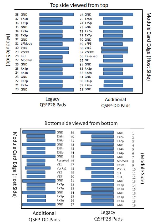
The QSFP-DD DR4 module edge connector consists of a single paddle card with 38 pads on the top and 38 pads on the bottom for a total of 76 pads. The pads are defined in such a manner so as to accommodate insertion of a QSFP module into a QSFP-DD receptacle.
|
PIN |
Logic |
Symbol |
Description |
Note |
|
1 |
|
GND |
Ground |
1 |
|
2 |
CML-I |
Tx2n |
CML-I Transmitter 2 Inverted Data Input |
|
|
3 |
CML-I |
Tx2p |
CML-I Transmitter 2 Non-Inverted Data Input |
|
|
4 |
|
GND |
Ground |
1 |
|
5 |
CML-I |
Tx4n |
CML-I Transmitter 4 Inverted Data Input |
|
|
6 |
CML-I |
Tx4p |
CML-I Transmitter 4 Non-Inverted Data Input |
|
|
7 |
|
GND |
Ground |
1 |
|
8 |
LVTTL-I |
ModSelL |
LVTLL-I Module Select |
|
|
9 |
LVTTL-I |
ResetL |
LVTLL-I Module Reset |
|
|
10 |
|
VCCRx |
+3.3V Power Supply Receiver |
2 |
|
11 |
LVCMOS-I/O |
SCL |
LVCMOS-I/O 2-Wire Serial Interface Clock |
|
|
12 |
LVCMOS-I/O |
SDA |
LVCMOS-I/O 2-Wire Serial Interface Data |
|
|
13 |
|
GND |
Ground |
1 |
|
14 |
CML-O |
Rx3p |
CML-O Receiver 3 Non-Inverted Data Output |
|
|
15 |
CML-O |
Rx3n |
CML-O Receiver 3 Inverted Data Output |
|
|
16 |
|
GND |
Ground |
1 |
|
17 |
CML-O |
Rx1p |
CML-O Receiver 1 Non-Inverted Data Output |
|
|
18 |
CML-O |
Rx1n |
CML-O Receiver 1 Inverted Data Output |
|
|
19 |
|
GND |
Ground |
1 |
|
20 |
|
GND |
Ground |
1 |
|
21 |
CML-O |
Rx2n |
CML-O Receiver 2 Inverted Data Output |
|
|
22 |
CML-O |
Rx2p |
CML-O Receiver 2 Non-Inverted Data Output |
|
|
23 |
|
GND |
Ground |
1 |
|
24 |
CML-O |
Rx4n |
CML-O Receiver 4 Inverted Data Output |
|
|
25 |
CML-O |
Rx4p |
CML-O Receiver 4 Non-Inverted Data Output |
|
|
26 |
|
GND |
Ground |
1 |
|
27 |
LVTTL-O |
ModPrsL |
Module Present |
|
|
28 |
LVTTL-O |
IntL |
Interrupt |
|
|
29 |
|
VCCTx |
+3.3V Power Supply Transmitter |
2 |
|
30 |
|
VCC1 |
+3.3V Power Supply |
2 |
|
31 |
LVTTL-I |
LPMode |
LVTLL-I Low Power Mode |
|
|
32 |
|
GND |
Ground |
1 |
|
33 |
CML-I |
Tx3p |
CML-I Transmitter 3 Non-Inverted Data Input |
|
|
34 |
CML-I |
Tx3n |
CML-I Transmitter 3 Inverted Data Input |
|
|
35 |
|
GND |
Ground |
1 |
|
36 |
CML-I |
Tx1p |
CML-I Transmitter 1 Non-Inverted Data Input |
|
|
37 |
CML-I |
Tx1n |
CML-I Transmitter 1 Inverted Data Input |
|
|
38 |
|
GND |
Ground |
1 |
|
39 |
|
GND |
Ground |
1 |
|
40 |
CML-I |
Tx6n |
CML-I Transmitter 6 Inverted Data Input |
|
|
41 |
CML-I |
Tx6p |
CML-I Transmitter 6 Non-Inverted Data Input |
|
|
42 |
|
GND |
Ground |
1 |
|
43 |
CML-I |
Tx8n |
CML-I Transmitter 8 Inverted Data Input |
|
|
44 |
CML-I |
Tx8p |
CML-I Transmitter 8 Non-Inverted Data Input |
|
|
45 |
|
GND |
Ground |
1 |
|
46 |
|
Reserved |
For Future Use, No Connect |
|
|
47 |
|
VS1 |
Module Vendor Specific 1, No Connect |
|
|
48 |
|
VCCRx1 |
+3.3V Power Supply Receiver |
2 |
|
49 |
|
VS2 |
Module Vendor Specific 2, No Connect |
|
|
50 |
|
VS3 |
Module Vendor Specific 3, No Connect |
|
|
51 |
|
GND |
Ground |
1 |
|
52 |
CML-O |
Rx7p |
CML-O Receiver 7 Non-Inverted Data Output |
|
|
53 |
CML-O |
Rx7n |
CML-O Receiver 7 Inverted Data Output |
|
|
54 |
|
GND |
Ground |
1 |
|
55 |
CML-O |
Rx5p |
CML-O Receiver 5 Non-Inverted Data Output |
|
|
56 |
CML-O |
Rx5n |
CML-O Receiver 5 Inverted Data Output |
|
|
57 |
|
GND |
Ground |
1 |
|
58 |
|
GND |
Ground |
1 |
|
59 |
CML-O |
Rx6n |
CML-O Receiver 6 Inverted Data Output |
|
|
60 |
CML-O |
Rx6p |
CML-O Receiver 6 Non-Inverted Data Output |
|
|
61 |
|
GND |
Ground |
1 |
|
62 |
CML-O |
Rx8n |
CML-O Receiver 8 Inverted Data Output |
|
|
63 |
CML-O |
Rx8p |
CML-O Receiver 8 Non-Inverted Data Output |
|
|
64 |
|
GND |
Ground |
1 |
|
65 |
|
NC |
No Connect |
|
|
66 |
|
Reserved |
For Future Use, No Connect |
|
|
67 |
|
VCCTx1 |
+3.3V Power Supply Transmitter |
2 |
|
68 |
|
VCC2 |
+3.3V Power Supply |
2 |
|
69 |
|
Reserved |
For Future Use, No Connect |
|
|
70 |
|
GND |
Ground |
1 |
|
71 |
CML-I |
Tx7p |
CML-I Transmitter 7 Non-Inverted Data Input |
|
|
72 |
CML-I |
Tx7n |
CML-I Transmitter 7 Inverted Data Input |
|
|
73 |
|
GND |
Ground |
1 |
|
74 |
CML-I |
Tx5p |
CML-I Transmitter 5 Non-Inverted Data Input |
|
|
75 |
CML-I |
Tx5n |
CML-I Transmitter 5 Inverted Data Input |
|
|
76 |
|
GND |
Ground |
1 |
Notes
1.QSFP-DD uses common ground (GND) for all signals and supply (power). All are common within the QSFP-DD module and all module voltages are referred to this potential unless otherwise noted.Connect these directly to the host board signal-common ground plane.
2. VccRx, VccRx1, Vcc1, Vcc2, VccTx and VccTx1 shall be applied concurrently. VccRx, VccRx1, Vcc1, Vcc2, VccTx and VccTx1 may be internally connected within the module in any combination. Each connector Vcc pin is rated for a maximum current of 1000 mA.
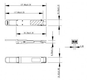
Mechanical Specifications

Figure 3. Mechanical Dimension (unit in mm)
ESD
This transceiver is specified as ESD threshold 1kV for SFI pins and 2kV for all other electrical input pins, tested per MIL-STD-883, Method 3015.4 /JESD22-A114-A (HBM). However, normal ESD precautions are still required during the handling of this module. This transceiver is shipped in ESD protective packaging. It should be removed from the packaging and handled only in an ESD protected environment.
Laser Safety
This is a Class 1 Laser Product according to EN 60825-1:2014. This product complies with 21 CFR 1040.10 and 1040.11 except for deviations pursuant to Laser Notice No. 50, dated (June 24, 2007).
Caution: Use of controls or adjustments or performance of procedures other than those specified herein may result in hazardous radiation exposure.
Revision History
| Revision | Date | Description |
| Preliminary | 2022/02/10 | Preliminary datasheet |


