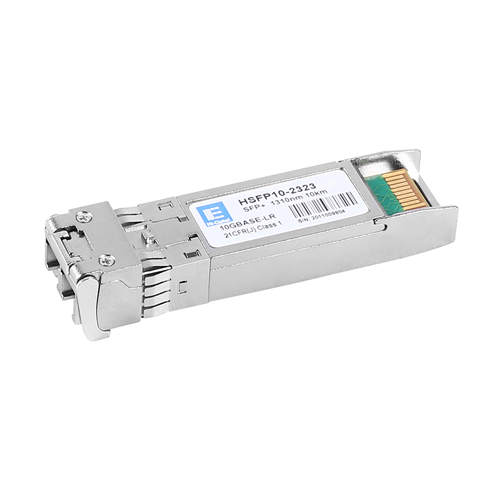
High Quality 10g Lr - 10GBASE-LR SFP+1310nm 10km Hi-Optel HSFP10-2323 module – Hi-optel
High Quality 10g Lr - 10GBASE-LR SFP+1310nm 10km Hi-Optel HSFP10-2323 module – Hi-optel Detail:
Descriptions
The transceiver consists of two sections: The high performance a 1310nm DFB Laser, Transmitter and high sensitivity PIN integrated with a TIA. Receiver.
A block diagram of the HSFP10-2323 SFP+ optical transceiver is shown below.

The module is hot pluggable into the 20-pin connector. The high-speed electrical interface is based on low voltage logic, with nominal 100 Ohms differential impedance and AC coupled in the module. The optical output can be disabled by LVTTL logic high-level input of TX_Disable. Loss of signal (RX_LOS) output is provided to indicate the loss of an input optical signal of receiver. The receiver RATE_SELECT pin is not used by the transceiver.
A 2-wire interface (SCL, SDA) is used for serial ID, digital diagnostics and other control /monitor functions.
● Absolute Maximum Ratings
| Parameter |
Symbol |
Min |
Max |
Unit |
| Storage Temperature |
TST |
-40 |
+85 |
℃ |
| Supply Voltage |
VCC3 |
0.0 |
+3.6 |
V |
| Relative Humidity |
RH |
5 |
95 |
% |
● Recommend Operation Environment
|
Parameter |
Symbol |
Min |
Typ |
Max |
Unit |
| Date Rate |
10.3125 |
11.3 |
Gb/s |
||
| Supply Voltage |
VCC |
+3.14 |
3.3 |
+3.47 |
V |
| Supply Current |
ICC |
300 |
mA |
||
| Power Dissipation |
PD |
800 |
1000 |
mW |
|
| Operating Temperature |
TOP |
-40 |
25 |
+85 |
℃ |
● Optical Characteristics (Condition: Ta=TOP)
|
Parameter |
Symbol |
Min |
Type |
Max |
Unit |
Note |
|
| Transmitter | |||||||
| Date Rate |
10.3125 |
11.3 |
Gb/s |
||||
| Optical Wavelength |
λ |
1260 |
1355 |
nm |
|||
| Average output power |
Po |
-6.5 |
0.5 |
dBm |
1 |
||
| Optical Extinction Ratio |
ER |
3.5 |
dB |
1 |
|||
| Optical Modulation Amplitude |
OMA |
-5.2 |
dBm |
||||
| Disabled Power | Poff | -30 | dBm | ||||
| Side Mode Suppression Ratio |
SMSR |
30 |
dB |
||||
| Dispersion penalty |
3.2 |
dB |
|||||
| Tx Jitter |
Txj |
Per 802.3ae requirements |
|||||
| Receiver | |||||||
| Date Rate |
10.3125 |
11.3 |
Gb/s |
||||
| Optical Wavelength |
λ |
1260 |
1355 |
nm |
|||
| Receiver Sensitivity |
R |
-14.4 |
dBm |
2 |
|||
| Receiver Sensitivity in OMA |
R |
-12.6 |
|||||
| Stressed Receiver Sensitivity in OMA |
R |
-10.3 |
dBm |
2 |
|||
| Maximum Input Power |
PMAX |
0.5 |
dBm |
||||
| LOS De-Assert |
LOSD |
-15 |
dBm |
||||
| LOS Assert |
LOSA |
-25 |
dBm |
||||
| LOS Hysteresis |
0.5 |
4 |
dB |
||||
| Receiver Reflectance |
-12 |
dB |
|||||
Notes
Note 1. Measured at 10.3125b/s with PRBS 231 – 1 NRZ test pattern.
Note 2. Under the ER worst case, measured at 10.3125 Gb/s with PRBS 231 – 1 NRZ test pattern for BER< 1×10-12
● Electrical Characteristics (Condition: Ta=TOP)
|
Parameter |
Symbol |
Min |
Typ |
Max |
Unit |
Note |
||
| Transmitter | ||||||||
| Differential input voltage swing |
VI |
150 |
1600 |
mVpp |
1 |
|||
| Common mode voltage tolerance |
15 |
- |
- |
mV |
||||
| Transmit Disable Input |
H |
VIH |
2.0 |
Vcc+0.3 |
V |
|||
|
L |
VIL |
0 |
0.8 |
V |
||||
| Transmit Enable Output |
H |
VOH |
2.4 |
Vcc+0.3 |
V |
|||
|
L |
VOL |
0 |
0.4 |
V |
2 |
|||
| Data Dependent Input Jitter |
DDJ |
0.1 |
UI |
|||||
| Data Input Total Jitter |
TJ |
0.28 |
UI |
|||||
| Input Differential Impedance |
Zin |
80 |
100 |
120 |
Ω |
|||
| Receiver | ||||||||
| Differential output voltage swing |
500 |
700 |
mVpp |
3 |
||||
| LOS Output |
H |
VOH |
2.4 |
Vcc+0.3 |
V |
2 |
||
|
L |
VOL |
0 |
0.4 |
V |
||||
| Rx Output Rise and Fall Time |
Tr/Tf |
30 |
ps |
20% to 80% |
||||
| Total Jitter |
TJ |
0.7 |
UI |
|||||
| Deterministic Jitter |
DJ |
0.42 |
UI |
|||||
| Output Differential Impedance |
Zon |
80 |
100 |
120 |
Ω |
|||
Note 1. TD+/- are internally AC coupled with 100Ω differential termination inside the module.
Note 2. Tx Fault and Rx LOS are open collector outputs, which should be pulled up with 4.7k to 10kΩ resistors on the host board. Pull up voltage between 2.0V and Vcc+0.3V.
Note 3. RD+/- outputs are internally AC coupled, and should be terminated with 100Ω (differential) at the user SERDES.
Pin Assignment
Diagram of Host Board Connector Block Pin Numbers and Name

Product detail pictures:

Related Product Guide:
"Based on domestic market and expand overseas business" is our development strategy for High Quality 10g Lr - 10GBASE-LR SFP+1310nm 10km Hi-Optel HSFP10-2323 module – Hi-optel , The product will supply to all over the world, such as: Bolivia, Ecuador, United Arab Emirates, Our products are very popular in the word, like South American, Africa, Asia and so on. Companies to "create first-class products" as the goal, and strive to provide customers with high quality products, provide high-quality after-sales service and technical support, and customer mutual benefit, create a better career and future!
We are long-term partners, there is no disappointment every time, we hope to maintain this friendship later!


