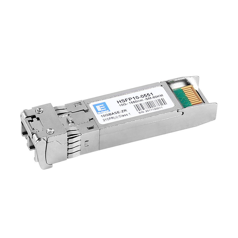
Reasonable price Cwdm Sfp 10g - 10GBASE-ZR SFP+ 1550nm 80km Hi-Optel HSFP10-0551 module – Hi-optel
Reasonable price Cwdm Sfp 10g - 10GBASE-ZR SFP+ 1550nm 80km Hi-Optel HSFP10-0551 module – Hi-optel Detail:
Descriptions
The SFP+ ZR module is small form factor pluggable module for duplex optical data communications such as 10GBASE-ZR/EZW defined by IEEE 802.3ae. It is with the SFP+ 20-pin connector to allow hot plug capability.
The transmitter input and receiver output impedance is 100 Ohms differential. Data lines are internally AC coupled. The module provides differential termination and reduce differential to common mode conversion for quality signal termination and low EMI.
The transmitter converts 10Gbit/s serial PECL or CML electrical data into serial optical data compliant with the 10GBASE-ZR standard. An open collector compatible Transmit Disable (Tx_Dis) is provided. A logic “1,” or no connection on this pin will disable the laser from transmitting. A logic “0″ on this pin provides normal operation. The transmitter has an internal automatic power control loop (APC) to ensure constant optical power output across supply voltage and temperature variations. An open collector compatible Transmit Fault (Tx_Fault) is provided. TX_Fault is a module output contact that when high, indicates that the module transmitter has detected a fault condition related to laser operation or safety. The TX_Fault output contact is anopen d rain/collector and shall be pulled up to the Vcc_Host in the host with a resistor in the range 4.7-10 kΩ.
TX_Disable is a module input contact. When TX_Disable is asserted high or left open, the SFP+ module transmitter output shall be turned off. This contact shall be pulled up to VccT with a 4.7 kΩ to 10 kΩ resistor.

SFP Module EEPROM Information and Management
The SFP+ modules implement the 2-wire serial communication protocol as defined in the SFP -8472.
The serial ID information of the SFP+ modules and Digital Diagnostic Monitor parameters can be accessed through the I2C interface at address A0h and A2h. The memory is mapped in Table 1. Detailed ID information (A0h) is listed in Table 2. And the DDM specification at address A2h. For more details of the memory map and byte definitions, please refer to the SFF-8472, “Digital Diagnostic Monitoring Interface for Optical Transceivers”.
Table 1. Digital Diagnostic Memory Map (Specific Data Field Descriptions)
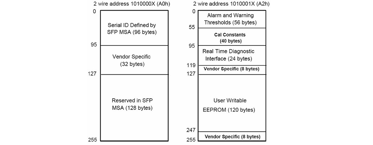
Table 2 – EEPROM Serial ID Memory Contents (A0h)
|
Data Address |
Length(Byte) | Name of Length |
Description and Contents |
| Base ID Fields | |||
| 0 | 1 | Identifier | Type of Serial transceiver (03h=SFP) |
| 1 | 1 | Reserved | Extended identifier of type serial transceiver (04h) |
| 2 | 1 | Connector | Code of optical connector type (07=LC) |
| 3-10 | 8 | Transceiver | |
| 11 | 1 | Encoding | 64B/66B (06h) |
| 12 | 1 | BR,Nominal | Nominal baud rate, unit of 100Mbps (67h) |
| 13-14 | 2 | Reserved | (0000h) |
| 15 | 1 | Length(9um) | Link length supported for 9/125um fiber, units of 100m |
| 16 | 1 | Length(50um) | Link length supported for 50/125um fiber, units of 10m |
| 17 | 1 | Length(62.5um) | Link length supported for 62.5/125um fiber, units of 10m |
| 18 | 1 | Length(Copper) | Link length supported for copper, units of meters |
| 19 | 1 | Reserved | |
| 20-35 | 16 | Vendor Name | SFP vendor name: Hi-Optel ECI |
| 36 | 1 | Reserved | |
| 37-39 | 3 | Vendor OUI | SFP transceiver vendor OUI ID |
| 40-55 | 16 | Vendor PN | Part Number: “HSFP10xxxxECI” (ASCII) |
| 56-59 | 4 | Vendor rev | Revision level for part number |
| 60-62 | 3 | Reserved | |
| 63 | 1 | CCID | Least significant byte of sum of data in address 0-62 |
| Extended ID Fields | |||
| 64-65 | 2 | Option | Indicates which optical SFP signals are implemented(001Ah = LOS, TX_FAULT, TX_DISABLE all supported) |
| 66 | 1 | BR, max | Upper bit rate margin, units of % |
| 67 | 1 | BR, min | Lower bit rate margin, units of % |
| 68-83 | 16 | Vendor SN | Serial number (ASCII) |
| 84-91 | 8 | Date code | Hi-Optel’s Manufacturing date code |
| 92 | 1 | Diagnostic type | |
| 93 | 1 | Enhanced option | |
| 94 | 1 | SFF-8472 | |
| 95 | 1 | CCEX | Check code for the extended ID Fields (addresses 64 to 94) |
| Vendor Specific ID Fields | |||
| 96-127 | 32 | Readable | Hi-Optel specific date, read only |
| 128-255 | 128 | Reserved | Reserved for SFF-8079 |
Table 2 – EEPROM Serial ID Memory Contents (A2h)
| Address | Bytes | Name | Description |
| 00-01 | 2 | Temp High Alarm | MSB at low address |
| 02-03 | 2 | Temp Low Alarm | MSB at low address |
| 04-05 | 2 | Temp High Warning | MSB at low address |
| 06-07 | 2 | Temp Low Warning | MSB at low address |
| 08-09 | 2 | Voltage High Alarm | MSB at low address |
| 10-11 | 2 | Voltage Low Alarm | MSB at low address |
| 12-13 | 2 | Voltage High Warning | MSB at low address |
| 14-15 | 2 | Voltage Low Warning | MSB at low address |
| 16-17 | 2 | Bias High Alarm | MSB at low address |
| 18-19 | 2 | Bias Low Alarm | MSB at low address |
| 20-21 | 2 | Bias High Warning | MSB at low address |
| 22-23 | 2 | Bias Low Warning | MSB at low address |
| 24-25 | 2 | TX Power High Alarm | MSB at low address |
| 26-27 | 2 | TX Power Low Alarm | MSB at low address |
| 28-29 | 2 | TX Power High Warning | MSB at low address |
| 30-31 | 2 | TX Power Low Warning | MSB at low address |
| 32-33 | 2 | RX Power High Alarm | MSB at low address |
| 34-35 | 2 | RX Power Low Alarm | MSB at low address |
| 36-37 | 2 | RX Power High Warning | MSB at low address |
| 38-39 | 2 | RX Power Low Warning | MSB at low address |
| 40-55 | 16 | Reserved | Reserved for future monitored quantities |
| Address | #Bytes | Name | Description |
| 56-59 | 4 | Rx_PWR(4) | Single precision floating point calibration data – Rx optical power. Bit 7 of byte 56 is MSB. Bit 0 of byte 59 is LSB. |
| 60-63 | 4 | Rx_PWR(3) | Single precision floating point calibration data – Rx optical power. Bit 7 of byte 60 is MSB. Bit 0 of byte 63 is LSB. |
| 64-67 | 4 | Rx_PWR(2) | Single precision floating point calibration data – Rx optical power. Bit 7 of byte 64 is MSB, bit 0 of byte 67 is LSB. |
| 68-71 | 4 | Rx_PWR(1) | Single precision floating point calibration data – Rx optical power. Bit 7 of byte 68 is MSB, bit 0 of byte 71 is LSB. |
| 72-75 | 4 | Rx_PWR(0) | Single precision floating point calibration data – Rx optical power. Bit 7 of byte 72 is MSB, bit 0 of byte 75 is LSB. |
| 76-77 | 2 | Tx_I(Slope) | Fixed decimal (unsigned) calibration data, laser bias current. Bit 7 of byte 76 is MSB, bit 0 of byte 77 is LSB. |
| 78-79 | 2 | Tx_I(Offset) | Fixed decimal (signed two’s complement) calibration data, laser bias current. Bit 7 of byte 78 is MSB, bit 0 of byte 79 is LSB |
| 80-81 | 2 | Tx_PWR(Slope) | Fixed decimal (unsigned) calibration data,transmittercoupled output power. Bit 7 of byte 80 is MSB, bit 0 of byte81 is LSB. |
| 82-83 | 2 | Tx_PWR(Offset) | Fixed decimal (signed two’s complement) calibration data, transmitter coupled output power. Bit 7 of byte 82 is MSB, bit 0 of byte 83 is LSB. |
| 84-85 | 2 | T(Slope) | Fixed decimal (unsigned) calibration data, internal module temperature. Bit 7 of byte 84 is MSB, bit 0 of byte 85 is LSB. |
| 86-87 | 2 | T(Offset) | Fixed decimal (signed two’s complement) calibration data, internal module temperature. Bit 7 of byte 86 is MSB, bit 0 of byte 87 is LSB. |
| 88-89 | 2 | V(Slope) | Fixed decimal (unsigned) calibration data, internal module supply voltage. Bit 7 of byte 88 is MSB, bit 0 of byte 89 is LSB. |
| 90-91 | 2 | V(Offset) | Fixed decimal (signed two’s complement) calibration data, internal module supply voltage. Bit 7 of byte 90 is MSB. Bit 0 of byte 91 is LSB. |
| 92-95 | 4 | Reserved | Reserved |
| Byte | Bit | Name | Description |
| Converted analog values. Calibrated 16 bit data | |||
| 96 | All | Temperature MSB | Internally measured module temperature. |
| 97 | All | Temperature LSB | |
| 98 | All | Vcc MSB | Internally measured supply voltage in transceiver. |
| 99 | All | Vcc LSB | |
| 100 | All | TX Bias MSB | Internally measured TX Bias Current. |
| 101 | All | TX Bias LSB | |
| 102 | All | TX Power MSB | Measured TX output power. |
| 103 | All | TX Power LSB | |
| 104 | All | RX Power MSB | Measured RX input power. |
| 105 | All | RX Power LSB | |
| 106 | All | Reserved MSB | Reserved for 1st future definition of digitized analog input |
| 107 | All | Reserved LSB | Reserved for 1st future definition of digitized analog input |
| 108 | All | Reserved MSB | Reserved for 2nd future definition of digitized analog input |
| 109 | All | Reserved LSB | Reserved for 2nd future definition of digitized analog input |
| Optional Status/Control Bits | |||
| 110 | 7 | TX Disable State | Digital state of the TX Disable Input Pin. Not supported. |
| 110 | 6 | Soft TX Disable | Read/write bit that allows software disable of laser. Not supported. |
| 110 | 5 | Reserved | |
| 110 | 4 | RX Rate Select State | Digital state of the SFP RX Rate Select Input Pin. Not supported. |
| 110 | 3 | Soft RX Rate Select | Read/write bit that allows software RX rate select. |
| Not supported. | |||
| 110 | 2 | TX Fault | Digital state of the TX Fault Output Pin. |
| 110 | 1 | LOS | Digital state of the LOS Output Pin. |
| 110 | 0 | Data Ready | Indicates transceiver has achieved power up and data is ready |
| 111 | 7-0 | Reserved | Reserved. |
| Byte | Bit | Name | Description |
| Reserved Optional Alarm and Warning Flag Bits | |||
| 112 | 7 | Temp High Alarm | Set when internal temperature exceeds high alarm level. |
| 112 | 6 | Temp Low Alarm | Set when internal temperature is below low alarm level. |
| 112 | 5 | Vcc High Alarm | Set when internal supply voltage exceeds high alarm level. |
| 112 | 4 | Vcc Low Alarm | Set when internal supply voltage is below low alarm level. |
| 112 | 3 | TX Bias High Alarm | Set when TX Bias current exceeds high alarm level. |
| 112 | 2 | TX Bias Low Alarm | Set when TX Bias current is below low alarm level. |
| 112 | 1 | TX Power High Alarm | Set when TX output power exceeds high alarm level. |
| 112 | 0 | TX Power Low Alarm | Set when TX output power is below low alarm level. |
| 113 | 7 | RX Power High Alarm | Set when Received Power exceeds high alarm level. |
| 113 | 6 | RX Power Low Alarm | Set when Received Power is below low alarm level. |
| 113 | 5 | Reserved Alarm | |
| 113 | 4 | Reserved Alarm | |
| 113 | 3 | Reserved Alarm | |
| 113 | 2 | Reserved Alarm | |
| 113 | 1 | Reserved Alarm | |
| 113 | 0 | Reserved Alarm | |
| 114 | All | Reserved | |
| 115 | All | Reserved | |
| 116 | 7 | Temp High Warning | Set when internal temperature exceeds high warning level. |
| 116 | 6 | Temp Low Warning | Set when internal temperature is below low warning level. |
| 116 | 5 | Vcc High Warning | Set when internal supply voltage exceeds high warning level. |
| 116 | 4 | Vcc Low Warning | Set when internal supply voltage is below low warning level. |
| 116 | 3 | TX Bias High Warning | Set when TX Bias current exceeds high warning level. |
| 116 | 2 | TX Bias Low Warning | Set when TX Bias current is below low warning level. |
| 116 | 1 | TX Power High Warning | Set when TX output power exceeds high warning level. |
| 116 | 0 | TX Power Low Warning | Set when TX output power is below low warning level. |
| 117 | 7 | RX Power High Warning | Set when Received Power exceeds high warning level. |
| 117 | 6 | RX Power Low Warning | Set when Received Power is below low warning level. |
| 117 | 5 | Reserved Warning | |
| 117 | 4 | Reserved Warning | |
| 117 | 3 | Reserved Warning | |
| 117 | 2 | Reserved Warning | |
| 117 | 1 | Reserved Warning | |
| 117 | 0 | Reserved Warning | |
| 118 | All | Reserved | |
| 119 | All | Reserved | |
| Byte | # Byte | Name | Description |
| 120-127 | 8 | Vendor Specific | 00h. |
Product detail pictures:
Related Product Guide:
"Based on domestic market and expand overseas business" is our development strategy for Reasonable price Cwdm Sfp 10g - 10GBASE-ZR SFP+ 1550nm 80km Hi-Optel HSFP10-0551 module – Hi-optel , The product will supply to all over the world, such as: Irish, Kyrgyzstan, United States, With excellent solutions, high quality service and sincere attitude of service, we ensure customer satisfaction and help customers create value for mutual benefit and create a win-win situation. Welcome customers all over the world to contact us or visit our company. We'll satisfy you with our qualified service!
As an international trading company, we have numerous partners, but about your company, I just want to say, you are really good, wide range, good quality, reasonable prices, warm and thoughtful service, advanced technology and equipment and workers have professional training, feedback and product update is timely, in short, this is a very pleasant cooperation, and we look forward to the next cooperation!

